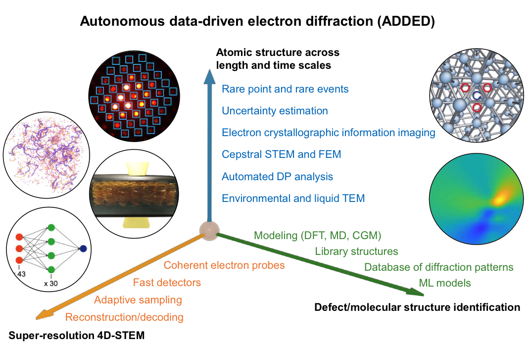
Electrons are charged particles that can be focused with magnetic lenses. When accelerated to high energies (~102 keV), they become ultra-fine probes with large scattering cross-sections, ideal for atomic resolution and nanoscale characterization, especially in nanoscience and nanotechnology. New detector and beam technologies on the horizon promise to deliver the electron beam and capture electron images on-demand with unprecedented speed and precision, generating massive datasets that could revolutionize how we understand interfaces, how we discover new materials with new functionality, and even how we do electron microscopy (EM). To capture these opportunities and position University of Illinois at the forefront of the revolution in electron microscopy, the Phase I team proposed to demonstrate the fast electron beam technology and smart electron imaging and to explore applications in the areas of interfacial coupling in bio-nano interfaces and grid energy storage and support-site interactions in single atom catalysts for fuel cell and carbon natural technology. Significant progress has been made with the GCOE SRI funding. This Phase II proposal seeks to expand the scope and size of the Phase I effort and develop Center-based proposals on interfacial materials science enabled by autonomous electron microscopy.
The envisioned autonomous electron microscopy is based on data-driven electron diffraction with extraordinary quantitative power and dynamic imaging capability, and thus potential to gain fundamentally new insights to address the long-standing questions outlined by Department of Energy and National Science Foundation. High-dimensional diffraction datasets (HDDs) will be collected using 4D-STEM (four-dimensional scanning transmission electron microscopy) techniques and machine-learning (ML) of these large datasets will be used for electron imaging. This approach, which is very different from traditional electron microscopy, will transform materials research and materials characterization. The proposed center aims to demonstrate autonomous electron microscopy for the identification and characterization of rare spatial and temporal features in real materials, especially interfaces, at the atomic scale.


